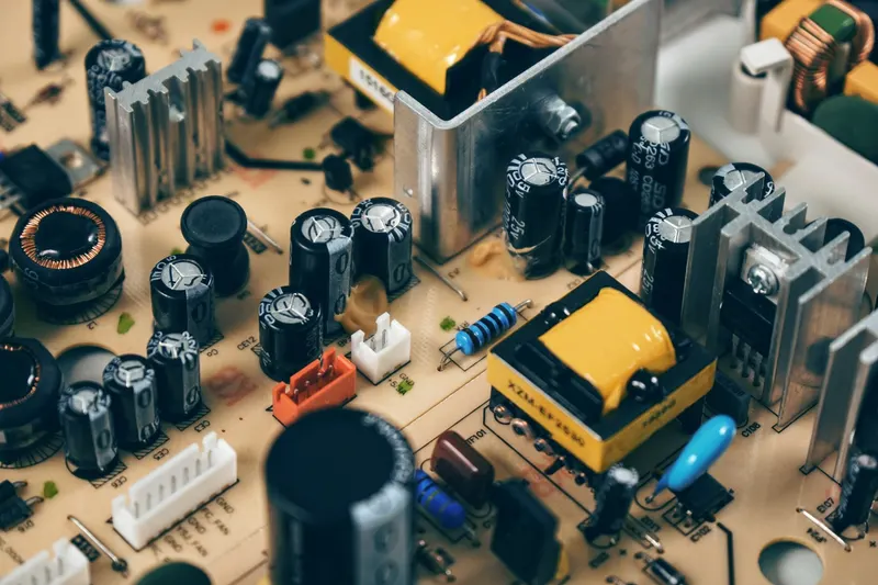
For the first half of the twentieth century, amplifying a weak electrical signal or switching a circuit on and off at high speed depended on the vacuum tube, also called a thermionic valve: a glass bulb containing metal elements in a near-vacuum. Tubes did enormous work in radio, long-distance telephony and the first electronic computers, but they had built-in drawbacks. A tube needed a heated filament to release electrons, so it drew power even when idle and gave off heat. Filaments burned out, glass cracked under shock, and each tube took up far more room than the signal it handled seemed to deserve. A machine with thousands of tubes needed large rooms, cooling and maintenance crews. Telephone engineers, who operated the largest electronic networks in the world, wanted a component that could amplify and switch without a filament, without a vacuum and with a long working life.
How it works
A transistor is built from a semiconductor, a material that conducts electricity better than an insulator but worse than a metal, and whose conductivity can be adjusted. The earliest transistors used germanium; silicon later became the dominant material. The adjustment comes from doping: adding tiny, controlled amounts of other elements to the crystal. Some dopants leave the crystal with extra mobile electrons (called N-type material). Others leave gaps where electrons are missing, known as holes, which behave like mobile positive charges (P-type material).
In the best-known early design, the bipolar junction transistor, three layers of alternating N and P material form a sandwich. A small current fed into the thin middle layer controls a much larger current flowing through the whole device. Used this way the transistor is an amplifier: a weak signal steers a strong one. It can also act as a switch. With no control current the path is blocked, and with control current it conducts. Repeated millions or billions of times, that on-off behavior is the basis of digital logic.
The field-effect transistor works on a different principle. A voltage on a control terminal, the gate, creates an electric field that changes how well a channel of semiconductor conducts. In the variant called the MOSFET (metal-oxide-semiconductor field-effect transistor), a thin insulating oxide layer separates the gate from the channel. The design draws very little power when idle and is well suited to being manufactured in huge numbers on one piece of silicon, which is why it became the main building block of modern integrated circuits.
Antecedents and the Bell Labs invention
The idea of controlling current inside a solid did not begin in 1947. Julius Edgar Lilienfeld filed patent applications for semiconductor field-effect devices from 1925, first in Canada and then in the United States, and the German physicist Oskar Heil patented a similar concept in Britain in 1934. Neither inventor is known to have demonstrated a working device with the materials available at the time, in part because crystals were not pure enough; some later reconstructions suggest that at least one of Lilienfeld's designs could have worked as described. Their patents matter as conceptual forerunners rather than as devices that shaped the Bell Labs effort.
The decisive effort was collective. At Bell Telephone Laboratories, the research arm of the American telephone monopoly AT&T, a solid-state physics group was assembled after World War II with the aim of finding a replacement for vacuum tubes and for the electromechanical relays used in telephone exchanges. The group brought together the theorist William Shockley, the experimentalist Walter Brattain and the theorist John Bardeen, along with chemists and metallurgists who prepared ever purer crystals. After studying how electric charge behaves on the surface of germanium, Bardeen and Brattain built the point-contact transistor. Two closely spaced metal points rested on a germanium crystal, and the device amplified a signal. The first working amplification is dated to December 16, 1947, and a demonstration for laboratory management followed on December 23. Bell Labs kept the work quiet for months and announced the device publicly at a press conference on June 30, 1948.
The name was chosen within the laboratory. John R. Pierce, a Bell Labs engineer, is credited with proposing it, and accounts describe a ballot among staff in 1948 in which his suggestion prevailed. It is generally explained as a blend of ideas such as transfer or transconductance and resistance, in line with device names such as varistor and thermistor; accounts differ slightly on the exact wording of the reasoning.
Shockley, who led the group, had not taken part in the first experiment. He reacted by working on a sturdier alternative and, in January 1948, conceived the junction transistor, filing a patent application that June. Working devices of this type were made around 1950, after advances in growing high-quality crystals, and Bell Labs presented the design publicly in 1951. The point-contact device was fragile and hard to reproduce, whereas the junction transistor proved more stable and easier to manufacture at scale. Bardeen, Brattain and Shockley shared the 1956 Nobel Prize in Physics for their research on semiconductors and their discovery of the transistor effect. Historians describe tension among the three over credit for the invention.
A parallel invention in France
In 1948 the German physicists Herbert Mataré and Heinrich Welker, working at Aulnay-sous-Bois near Paris for a French subsidiary of Westinghouse, independently developed a point-contact device they called the "transistron." Mataré had encountered related semiconductor effects in wartime work on crystal detectors for radar. Some accounts report consistent amplification in their laboratory in June 1948, around the time of the Bell Labs announcement; their French patent application is dated August 13, 1948, and the device was presented to the French press in May 1949. The episode shows that the problem was ripe: several teams with similar materials and knowledge reached close results by separate routes.
From laboratory to factory
AT&T held seminars and licensed transistor technology to many companies for a modest fee. A legal backdrop helped. The company was under antitrust pressure from the U.S. government, and a consent decree signed in January 1956 required it to license its existing patents and to stay within regulated telecommunications. Wide sharing of know-how sped up development across many firms.
Germanium had a weakness: its performance degrades as temperature rises. In 1954 Texas Instruments, with Gordon Teal leading the crystal work, made its first silicon transistor in April and announced at a May conference that silicon devices, which tolerated heat much better, were available commercially. In the same year, a pocket radio called the Regency TR-1 was announced in October and went on sale in the United States in November, reported as the first commercially produced transistor radio. It used four germanium transistors, was developed by Industrial Development Engineering Associates and marketed under the Regency name, and its transistors were supplied by Texas Instruments. Soon afterward the Japanese company that later became Sony brought out transistor radios of its own. These products carried the transistor to consumers and helped turn the radio into a portable personal object (see radio and wireless transmission).
In 1956 Shockley set up a company in California to commercialize transistors. In 1957 eight of his engineers left and founded Fairchild Semiconductor. In 1959 Jean Hoerni of Fairchild developed the planar process, which builds components on a flat silicon surface protected by an oxide layer. He had sketched the idea in late 1957 and demonstrated a working planar transistor in March 1959; Fairchild sold its first planar transistor in 1960. The process made production more reliable and laid the groundwork for integrated circuits. Also around then, Mohamed Atalla and Dawon Kahng at Bell Labs made the first successful silicon MOSFET. It was achieved in 1959 and demonstrated in 1960, so sources variously give either year.
Impact and limitations
The transistor made possible smaller, sturdier, lower-power devices: hearing aids, portable radios, military and space electronics, telephone exchanges and, above all, computers. Transistorized computers of the late 1950s were more reliable and needed less power and cooling than tube machines (for the earlier generation, see from mechanical calculators to the first computers). Falling costs per component built an industry and a region whose informal name, Silicon Valley, points to the material.
There are limits. Transistors dissipate heat, and packing more of them onto a chip runs into the problem of removing that heat. As dimensions approach a few atoms, quantum effects such as current leakage make the devices harder to control, and the cost of advanced factories rises with every generation. The industry has responded with new materials and transistor geometries, but the historical pace of miniaturization is not guaranteed to continue, and forecasts about it should be read as hypotheses.
A caution about interpretation is also in order. The transistor did not replace the tube overnight. Tubes stayed in use for decades in high-power transmitters, some audio amplifiers and specialized equipment, and they survive in niches today.
Connections to other technologies
The most direct line runs from the transistor to the integrated circuit, which fabricates many transistors and their wiring on a single piece of silicon. That integration in turn made the personal computer and other devices with compact processors practical. The story also ties to radio, the first mass consumer market for the component, and to the first computers, which needed thousands of dependable electronic switches.